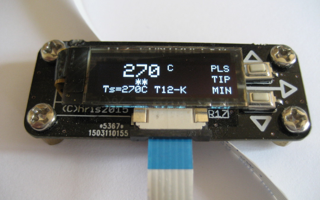
Somewhere in 2014 my interest was sparked by cheap Hakko T12 soldering tips available on e-bay. Those soldering tips are a whopping 70W which is far more then the 25W iron I got. Also the variety of tip shapes is amazing. For every soldering job from a delicate chip to large pins with large thermal mass, a tip is available. On a forum someone posted the basic info how to drive such a soldering tip. The basic idea behind them is relative easy. These tips have three terminals of which one is directly connected to the tip for ESD purpose. The other two terminals are connected to the heater inside (electrically isolated from the tip). In series with the heater there is a thermocouple which can measure the tip pretty accurately. The heater is powered for a (fixed) period and then powered off, during the off time the thermocouple voltage is measured. Process is repeated continuously and a control loop tries to reach (and maintain) the temperature that is required.
At some time I found a simple schematic of a cheap (Chinese) analogue controller and adapted it to be controlled by a microcontroller. I quickly threw together a schematic around a Microchip PIC microcontroller and a small OLED display. Main design constraints at that time were:
- must fit into 5x5cm PCB
- two separate boards (UI and controller board)
- onboard 1M ohm resistor for ESD
- tip detection
- power down/sleep mode
- controlled by a microcontroller
I start the design with a PIC12f1822 which is a feature rich 8 pin microcontroller. The PIC12 has a bigger brother which has 6 more pins. The idea at that stage was to have a basic temperature controlled design with an OLED and a few buttons. If more features where needed like power down input the bigger pic16f1823 could be soldered in. Later on I decided to skip the dual chip totally and just go for the pic16f1823. I assumed (which is a very evil thing :)) that both PICs were pin-compatible. Unfortunately that wasn’t the case and all the connections were wrong. Luckily with some bodge wire I could whip up a working prototype and test the basic workings. I also had some issues with the OLED which I though was a SSD1306 but it appeared to be a SH1106 (never trust the Chinese product descriptions). Both chips are very similar but have some quirks/differences. Most of the differences were the way the display is wrapped and the initialization. After some google-fu and some hours coding later I had the display working the same way as SSD1306 (and made it selectable with a #define in the code).
I corrected the errors with the pin out and send off the new revision of the PCB to China. The second revision also added some protection resistors in the power down and tip signals to make it more robust. Electrically the PCB was fine now and I was confident about its workings. The layout of the components was ok, but I realized it was only suitable for soldering by hand. At that time I showed it off in China and the people there convinced me to start a small production run. I realized if I wanted it to be manufactured, I need to change a few things. the biggest issue was the placement of the flatflex connectors. In the original design they were facing to each other and impossible to pick and place (too less space). You need to separate the board before soldering them down. Even if it was possible to solder them this way the boards couldn’t be tested properly as the cable can’t be connected and without testing selling could be a very risky business.
Later revisions consist of some silkscreen issues (still some are left :/), adding a ICSP (In Circuit Serial Programming) and a fools diode on the input. Probably other revisions will follow, but for now I think it is fine :). More info here about the project.
