I usually collect a few PCB designs before sending them off to the PCB fabhouse. I prefer to use dirtypcbs.com as I know Ian from dangerousprototypes.com for a long time and think he provides good quality, and fast turn around time for your money. Also tend to be loyal to my suppliers so a better alternative may exist. The main reason I wait before sending them off is that I want my PCBs returned quickly. DirtyPCBs provide fast DHL shipping (about 2-3 days to .nl) but it is quite expensive (about 30 USD) compared to the manufacturing the PCBs. Luckily the PCBs don’t weight a ton, and adding more designs will not add much additional shipping costs.
Most time of the PCB designing process goes into the design of the schematic and the routing of the PCB. Adding components to your library is usually a small task which don’t take much time. Nowhere in the process of designing the PCB this small but very important step is checked again. So make sure that the footprints and pinout is correct and double, tripple and quadriple check it!! The easist way to check the footprint (and PCB) is to print it on a sheet of paper (make sure the scale is 1:1 and not mirrored!) Place the component(s) on the printed page and check if all the printed pads align with the components and whether there is plenty of extra copper around it to be handsoldered. Next make sure the placement part of silkscreen is making sense. To check the pinout I found it usefull to enable pins numbered in the cad package and check it with the datasheet afterwards. Preferable dont check it on the same day as you made the library part as you probably make the same mistake again.
Generating Gerber is luckily an automated process, but also prone to lots of errors. enabling the wrong layer(s) in the copper or silkscreen layer could easily ruin your day. PCB manufacturers produces exactly what you tell them to do, nothing more and nothing less, so it is always your own fault. There are several options to check if the gerbers are what you expect. I personally use circuitpeople.com, which is an online tool to check your gerbers. You can upload the same .zip file to them as you would send your boardhouse. They show how each of the layer (copper bottom, top, silkscreen bottom, top, board outline and drill) looks like. Only if you have double checked them send them off.
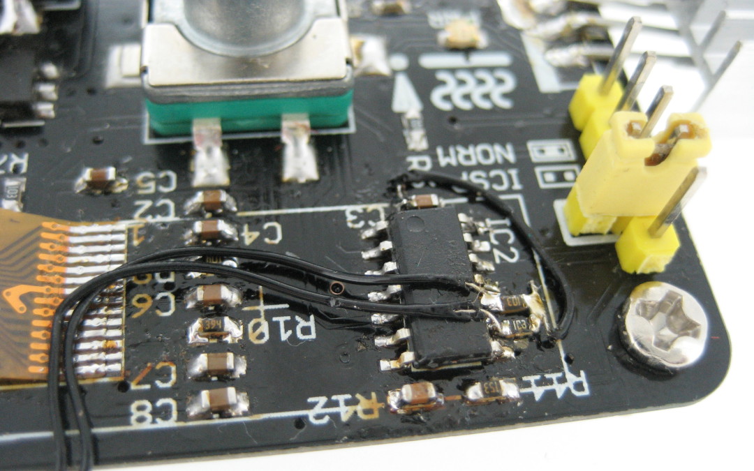
Other things that could go wrong is swapping signals like RXD/TXD, MOSI/MISO and SDA/SCL. These signal are alway ‘seen’ to or from a device, so an error is easily made. To avoid this you can add these names to the pins of the devices in the library, i.e. RA4/TX and RA5/RX. On prototypes these errors can be easily fixed (on the prototype) with some thin wire (I prefer wirewrap wire for that) and lots of patience. Other errors you can make is to forget to add required components, like pullups on an I2C bus or capacitors on a crystal, or selecting the wrong footprint like D2PAK instead of DPAK and a too small SOIC8 (150mil) for a SPI memory.
Bottom line is to check very often and if possible let other people check it too. In a few days I’ll do a post (or two) how to correct these silly mistakes.

Wooohoo! All good tips. Keep it up Sjaak.
Nice write up !
Also one important addition from my experience:
Check the pin assignments in your final layout against the datasheets and not against your own notes.
I usually take a lot of notes while designing things, since I don’t want to jump from datasheet to datatsheet all the time.
When I ordered my very first pcb that was not designed for etching myself, I was lazy and checked against my notes, which had mixed up RX/TX for a ft232rl.
And as small side note: “MOIS” – “Master Out In Slave” … never heard of that pin.
thanks and fixed!
mosi/miso are the best names for i/o pins, because you always know how is the master and who is the slave and what they are doing, transmitting or receiving, but the tx/rx are the worst, sda/scl are ok, but only if you put the pull-up resistors on them 🙂
Keep tracks as thick as possible, and spacing as high as possible.
Smaller tracks may be supported by the manufacturer, but if you need to make changes the extra track thickness will make the wirewrap jumpers easier to install.
Mostly I design the regular (non-power) tracks 10 mil and 16 mil for power. Spacing is (mostly) 25. It seems ok-ish to repair with wirewrap wire. I don’t want to design for repair but design for manufacture 😛
I’ve started putting “patch areas” next to my connectors, since I know that no matter how many times I check the pinout, some of them will be reversed. It’s basically two pin holes connected with a trace. If needed, it’s easy to cut the trace and solder wires into the holes. The downside is that this can eat a whole lot of board space, but you can use eg. SMD pads to achieve the same effect, just not as neat.
Another thing I learned the hard way is that a connector’s footprint on the board can be larger than what you see in the CAD tool (eg. a shrouded pin header), so make sure to check the dimensions in the mechanical drawings. Also, if the board is meant to be hand-soldered, make sure it’s actually possible, and try to avoid hard ordering dependencies (“R53 has to be soldered before C4 and C8, or you can’t access the pads”).
Ever though of not soldering in the connector and use fly wires? It depends on the type op connector (should be pth) 🙂
I don’t know which CAD software you used but EAGLE for example has the keepout layer. You can put the outline of the shrouded header in there. If there are components in this area the DRC would give an error. I suspect other CAD packages has the same capabilities.
To make a board (more) handsolderfriendly use slightly larger pads and make them longer. Alternative is to use solderpaste on the hard to solder packages and hotair them.
However it still all comes to the quality of the footprints in the library.
Here’s my checklist (derived after sooo many screw ups)
schematic check
erc
look for cross-sheet references that aren’t connected
add 2 fudicials, sparkfun lib-FIDUCIAL-1X2
4 mounting holes
add ground test points with holes for probe gnd
check notes.txt file for todos
create readme.txt with board name, zip content desc and fudicial placement, example below
check that all operational output lines have pull up/down during reset
make sure I2C SDA/SCL have pull-up resistors and solderable test points
board check
put a silk square down for sharpie id marking
add dimensions to tDocu
load dru file, this sets spacing for pours, etc
ratsnest
load board house’s dru then drc
ratsnet then run zoom-unrouted
add company name to tNames
add board name and version to tNames
run normalize-text:
set to 40 & 8 mils
smashes all components
place names with top, bottom off, tcream on
place logo with import-bitmap, or use lib part logo-oshw
check all the version numbers, board, schematic, readme and zip filename (to be created)
board submission
print layout
check connector placement
create readme.txt with fudicial placement
cam 4 layer
gerb274x-4layer.cam
make sure layer 51 tDocu is in plc, side silkscreen CMP
make sure layer 200 bmp is in plc, side silkscreen CMP
excellon.com
gerbv *.crc *.plc *.stc *.cmp *.ly2 *.l15 *.sol *.sts *.pls
run Centroid_ScreamingCircuits_smd.ulp
update version and rev in readme.txt, add version/rev to sheet 1 of sch
zip gerber.zip *.cmp *.crc *.crs *.drd *.dri *.gpi *.l15 *.ly2 *.plc *.pls *.sol *.stc *.sts readme.txt *centroid.csv *.dim
zip -sf gerber.zip
verify that sch and brd are NOT included in gerber zip file
mv gerber.zip to board-v0.0-gerber.zip
print sch and brd as pdf
zip board-v0.0-release.zip board-v0.0-gerber.zip *.sch *.brd *.pdf *.pdf *.csv
mv 2 zip files to ../release dir
freedfm
cat > readme.txt << EOF
This information, board files, assembly instructions and bill of
materials are company confidental.
Not for distribution.
board
???
version
???
date
???
svn revision
???
fudicials at
x,y
x,y
2 layer description
2 layer board
crc component cream
plc component side silkscreen
stc component side solder stop mask
cmp component side copper
sol solder side copper
sts solder side solder stop mask
pls solder side silkscreen
crs solder cream
drd drill data
dri drill info
gpi gerber info
2 layer stack up sequence
top x.cmp
bottom x.sol
4 layer description
4 layer board
crc component cream
plc component side silkscreen
stc component side solder stop mask
cmp component side copper
ly2 layer2
l15 layer15
sol solder side copper
sts solder side solder stop mask
pls solder side silkscreen
crs solder cream
drd drill data
dri drill info
gpi gerber info
4 layer stack up sequence
top x.cmp
inner 2 x.ly2
inner 3 x.l15
bottom x.sol
2 layer description – using itead's cam
Silk Top: pcbname.GTO
Solder Stop Mask Top: pcbname.GTS
Top layer: pcbname.GTL
Bottom layer: pcbname.GBL
Solder Stop Mask Bottom: pcbname.GBS
Silk Bottom: pcbname.GBO
NC Drill: pcbname.TXT
Drill Board Outline: pcbname.do
Edge Milling: pcbname.GML
Pad Mask Bottom: pcbname.GBP
Pad Mask Top: pcbname.GTP
2 layer stack up sequence
top x.GTL
bottom x.GBL
contact info
firstName lastName
phone number
email
EOF
I got bit by this on the first board I sent out to DirtyPCBs as well. I swapped the Drain and Gate pins on the MOSFETs on the board.
Worked fine on the toner transfer version, I re-laid out the board, and somehow messed it up.
To punish myself, I ordered the next set of boards *without* fast shipping.
🙂
Woo that was harsh for yourself. Never order PCBs without fast shipping 🙂
When a friend of mine and I ordered our first batch at DirtyPCB’s we made that exact same error… We rushed a little into it and made ourselves to order them that same night, big mistake ofcourse. We should have slept on it for a night to check everything with a fresh pair of eyes….
Thankyou for your writeup Sjaak! I’ll readup on your other blogposts as well. Keep up the good work.
Greetings from the sunny Southern parts of NL 😉