Recently I got a voucher to try Seeed PCB manufacturing, and decided to compare them to my regular PCB manufacturer DirtyPCBs.com. It is always nice to have an alternative to an existing supplier. At first glance they look very similar but some (small) differences exist. Let me introduce them both to you:
Seeedstudio
Eric Pan started Seeedstudio back in 2009/2010 and offered various services like manufacturing PCBs and fulfillment . AFAIK they were the first offering 2 layer, professional looking PCB service for a hobbiest friendly price (I think it cost back then 25USD for 5×5 cm PCB without shipping). At the time of ordering they offered 2 layer 7cmx7 for 9.95 USD (+8.33 USD shiping to NL) or 10x10cm for 14.95 USD (+8.33 USD shipping to NL). At the time of writing this article the price has dropped to 9.90 8.91 USD for 10x10cm. Standard design rules are 6/6 mil and 0.3mm holes, but can be extended at a cost (unfortunately it tends to add up quickly), and panelizing multiple designs is not allowed but can be bought at 10 USD per extra design in the panel, also adding extra costs rapidly.
Dirtypcbs.com
Dirtypcbs started out as a nonsense gateway to cheap Chinese PCB manufacturing (and other services like 3D printing or assembly) for just a small group of friends from Ian Lesnet. The interface is a page where you upload the design and everything is automatic from there on. The system is designed to be simple and handle most user interaction without human admin interaction. Users can update the board files or properties (if not sent of the board house), cancel their order before it goes into production. The board houses DirtyPCBs are using are quite forgiving in panelizing (as long as the panels are connected it is ok) and the designrules are quite relax(12 mil holes and 5/5 6/6 mil routing). Also their pricing is simple: designs under 5x5cm are 14 USD or under 10×10 25 USD with worldwide shipping included. However shipping worldwide can take up to 6 weeks, luckily they offer also DHL shipping. This is a bit more expensive, but the extra charge for an other PCB is very small so quite reasonable. I like my PCBs in fast! 😉
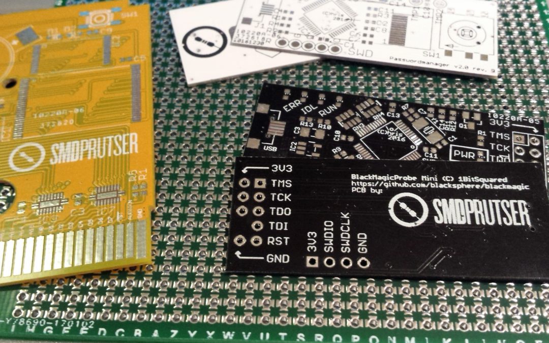
PCB from Seeed
The PCBs came out great and the silkscreen looks quite sharp. The silkscreen was a bit off (the outlines for placement of components) but IMHO acceptable for prototype quality PCB and DirtyPCB also suffers the same problem. In general the PCBs looks clean and without any visible problems. The HASL finish is a bit thick to my tast and in some places it is more a blob then a small layer. They don’t seem to be e-tested (no markings on the side nor distinct e-test dimples on the pads). I contacted their tech support and they assured they etest all their PCBs! Looking under a microscope reveals the pits, perhaps the thick HASL finish has obscured them. I preferred they had marked the PCBs though.
PCB from DirtyPCBs.com
The silkscreen looks a bit more grainy and seems to be printed by an inkjet and a bit more thicker/fatter then the Seeed PCB. Hoever the HASL finish is thin and pleasant. All boards are e-tested and have no visible problems too. Silkscreen is also a bit off, but still acceptable for prototypes.
Final verdict
Both services are great for hobbyist use and offer comparable quality. DirtyPCB is a bit cheaper and more flexible then Seeed and also offers DHL for people without a VAT number. With their protopack offer you can end up with an extra board or two. On the other side Seeed offers also lots of other stuff, like breakout boards, which can make a combined shipping more attractive and they offer better PCBs (i.e. tighter spacing or smaller holes) at more cost. Personally I think each supplier have a different audience but most of my designs would be fit in the DirtyPCBs offer, but I like to have an alternative if I have more fancy demands.

I like the service from Elecrow: https://www.elecrow.com/services/pcb-prototyping.html
They have similar offerings, but additionally 5 pcs 10 cm x 5 cm for 9.50$ + 5$ tracked shipping. Free solder mask color choice and different board thickness, also no additional costs. Although the offer says 5 pcs, they regularly send 10 🙂